Body Biasing Injection experiments
Published on 05 October 2021
Several months ago, I stumbled upon this paper from Colin O’Flynn. Since I never heard about this technique, I thought it could be interesting to try it by myself and see how it performs.
Body Biasing Injection
Body Biasing Injection has first been presented in this paper from P. Maurine et al. The rough idea is to inject a high voltage pulse directly on the backside of the silicon of the target chip in order to generate faults.
The induced voltage bias will modify the threshold voltage of the underlying transistors and can potentially prevent some bits to be correctly forwarded through the CPU circuitry.
The main advantage of this technique compared to voltage glitching for instance is that it is more localized and can only perturbate a specific region of the target chip.
Several other papers are covering this technique:
- Yet Another Fault Injection Technique : by Forward Body Biasing Injection by P. Maurine et al.
- Body Biasing Injection Attacks in Practice by Noemie Beringuier-Boher et al.
Before we dig deeper, let's review the basics about chips. The die is a silicon substrate where several layers of metal are applied in order to create a circuit containing billions of transistors. The following picture from Wikipedia shows the different layers in a die:
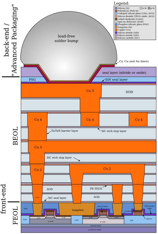
When talking about different injection techniques, the terms frontside and backside are often used. Contrarily to the schematic above:
- The frontside is the metal side of the die. It's the one connecting the die pad to the actual chip package pins
- The backside is the silicon side of the die. It is basically the other side of the silicon substrate.
Building the injector
In all of these papers, a high voltage generator was used and coupled with a pulse generator in order to generate the pulses. This kind of equipment is generally quite complicated to use, so Colin O’Flynn took a different approach by using a transformer in order to generate a high voltage spike.
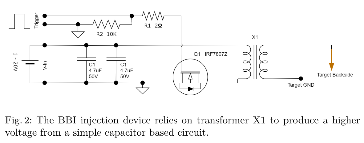
The MOSFET Q1 is used to quickly drop the voltage across the primary of the transformer. This will generate a voltage spike on the secondary coil, proportional to the number of turns ratio between the primary and the secondary of the transformer.
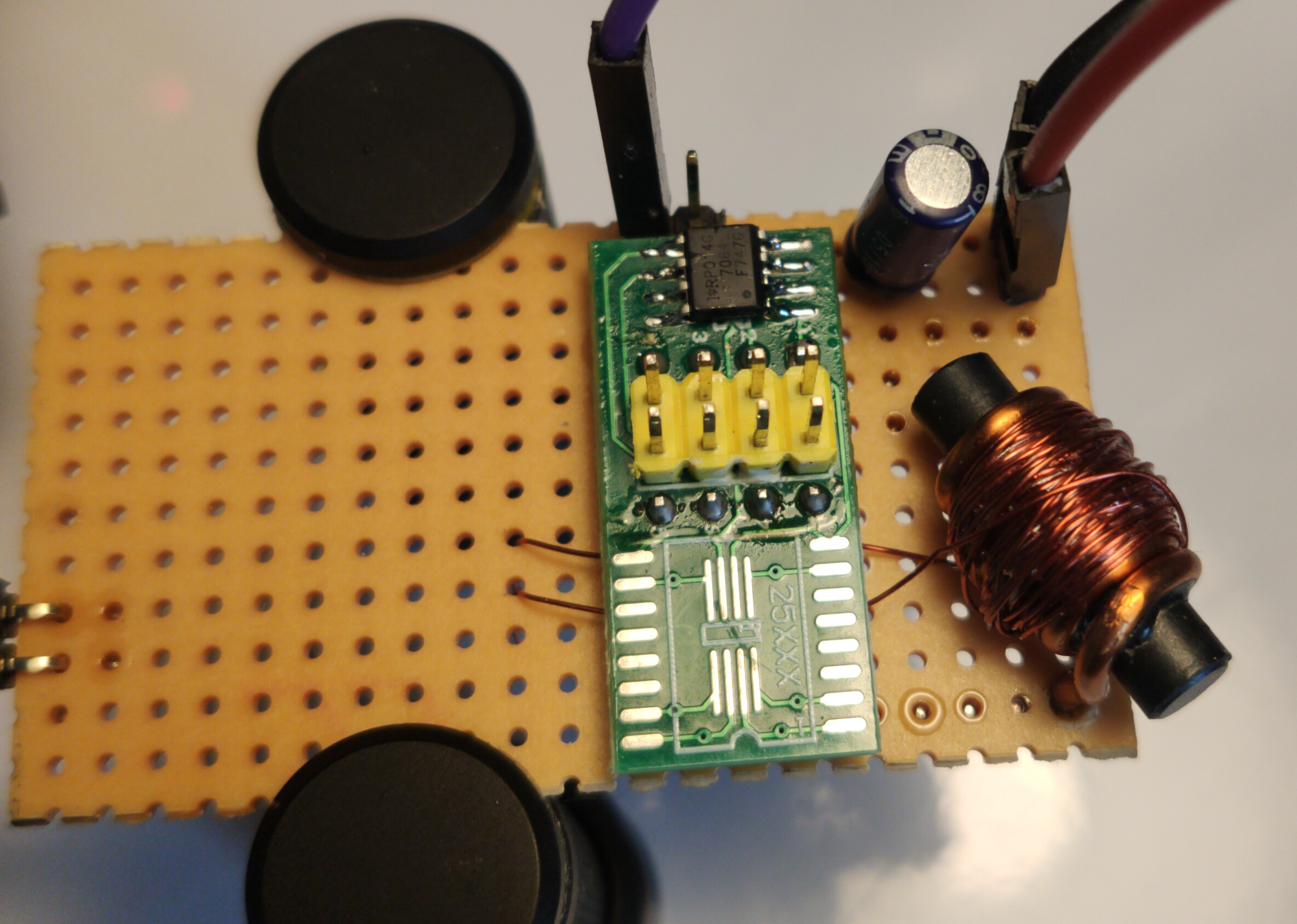
I built my own version of the BBI injection by using scrape parts I found around my desk.
- The two capacitors have been replaced by a single 100μF capacitor.
- The MOSFET I used is a IRF7470
- The transformer is a 6 turns inductance I recycled from a dead motherboard. I wound 60 turns of 0.2mm wire to make the secondary.
- The injection probe is a simple spring loaded pogo pin. This will be important later on.
In the end, the injection probe looks like this:
Testing the probe
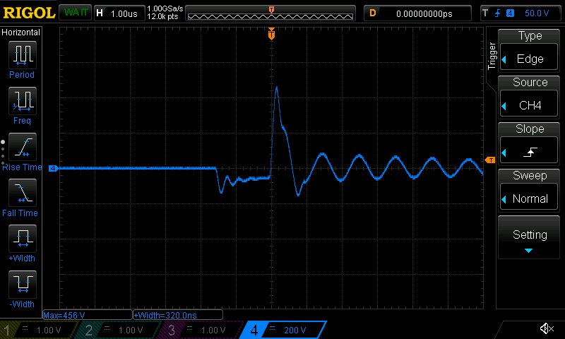
As the turn ratio on the transformer is 1:10, a 1V input should generate a 10V spike on the secondary. Hooking up the oscilloscope directly on the output could be dangerous with standard probes, as the voltage could kill the input. I used a 100:1 passive probe that is able to withstand up to 1200V in order to be able to take measurements.
The width of the MOSFET gate pulse changes the shape and height of the pulse, so I tested various gate pulse widths and fixed the pulse width to 1.5μs, which provides the highest voltage spike.
Here is an example output pulse using 10V input voltage and 1500ns gate pulse:
and with 1V input voltage and 1500ns gate pulse:
Interestingly, the assumed turn ratio of 1:10 does not look correct at all (thanks to the high voltage probe, my oscilloscope is still safe). I am not sure about what is happening here, but my explanation is that the different coil wire diameters plays a role. The approximate ratio is measured around 1:50 instead of 1:10.
Update 10/27/2021 As mentioned by @WestonBraun:
You are getting a much higher voltage from your pulse generator because the
transformer is not clamped, it's acting like a flyback transformer
https://en.wikipedia.org/wiki/Flyback_converter

In your waveforms there is a negative pulse closer to what you would expect
before the HV pulse.
Thanks to him for that information.
Bench preparation
Preparing the target
As a test target, I took a STM32F103 Nucleo devkit I had lying around. The chip is a STM32F103RBT6 which is quite common.
As BBI requires physical access to the backside, we need to grind through the plastic case of the chip in order to reach the silicon. However, there's a catch here: The silicon side of the die is located on the back of the chip package. We therefore not only need to grind the back side of the chip, but also dig a hole in the PCB in order to place the injection probe.
Looking at the schematics for the devkit shows that the PCB under the chip does not contain any important signals but only some GPIO traces to the headers, it is therefore possible to drill through the PCB and only loose some GPIOs. After that, grinding the chip is a matter of patience and precision. Note that you can grind the silicon a bit without harming the chip.
Once done, the board looks like this (the image shows a probe placed on the silicon as well).
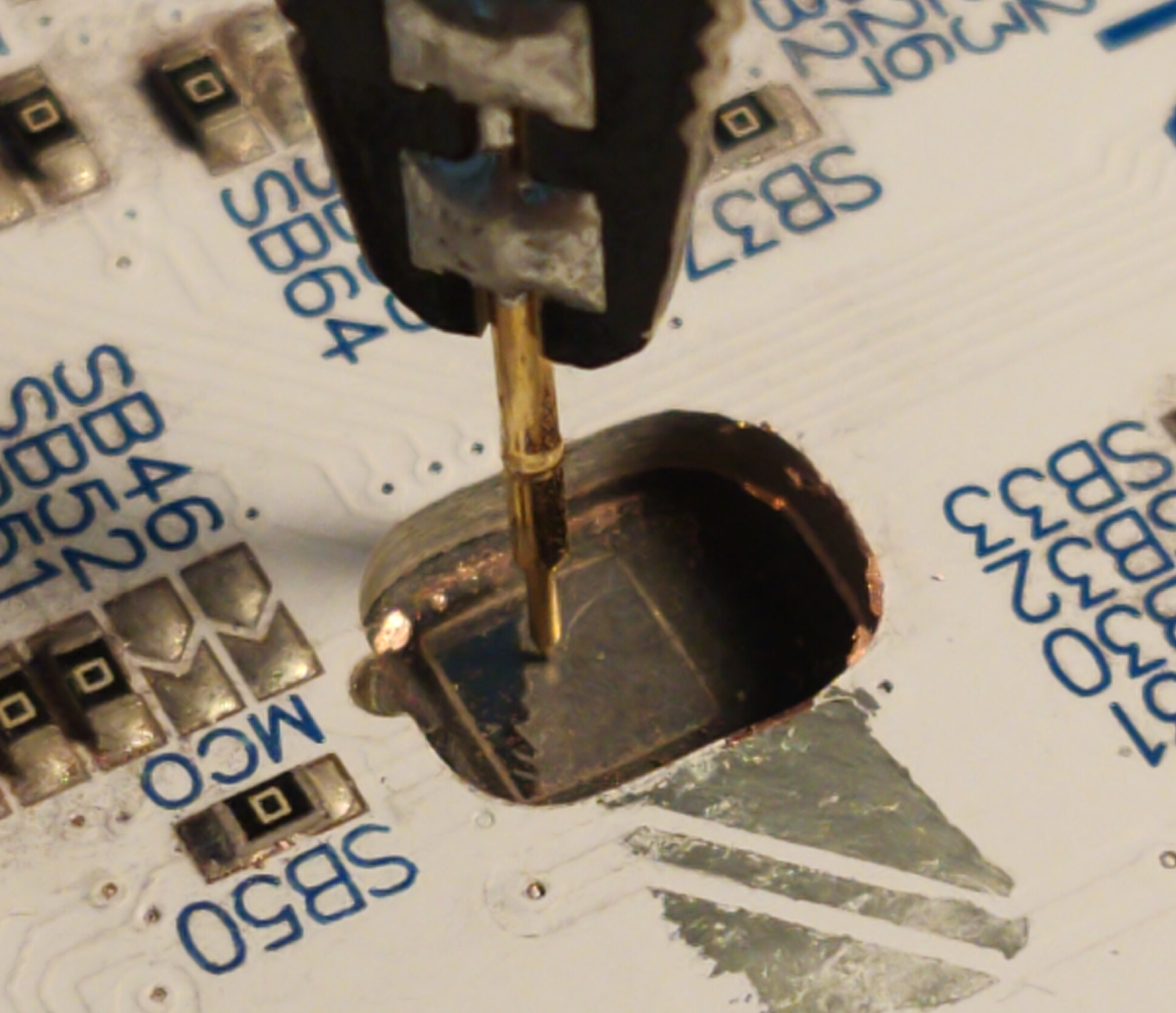
One interesting thing to notice is that this chip's die has a copper pad glued to the silicon. This pad can be removed using a scalpel to avoid breaking the die. You can see that the left part of the silicon looks smooth, this is because I was able to tear apart the last part of the copper pad that was glued here.
Once the device has been prepared, we can verify that there is a resistance value between the silicon and the ground. By using a multimeter, I could measure this resistance to be between 90kΩ and 240kΩ depending on the measurement point on the die.
Preparing the XYZ table
In order to move the probe accurately across the die, a XYZ table is required. However, it is possible to use a 3D printer to get the same kind of results. I soldered the pogo pin to a piece of prototype board and a SMA connector and fixed this small PCB to the 3D printer head using a 3D-printed part.
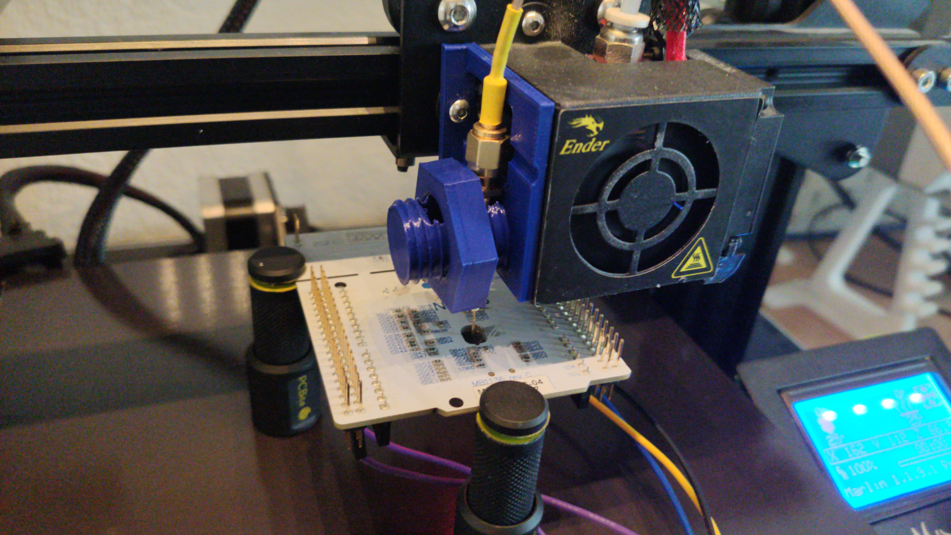
My friend Azox prepared a Python library that can be used to drive the printer and scan a whole area using a few Python commands:
from glitch3d import printer
from glitch3d import chip

# Prepare the printer and set its zero position
ender = printer(port="/dev/ttyUSB5",baudrate=115200, timeout=1)
ender.load_settings("glitch3d/settings/ender3.ini")
ender.set_pos(0,0,10)
ender.go_home_xyz()

# Prepare the area to scan with 0.2mm steps
target = chip()
target.set_home(166,76.5)
target.set_end(168.7,79.8)
target.steps=0.2

#Define Z axis positions in order to move the probe
UP = 76
DOWN = 73

# Run the scan. Try to inject a glitch for every position
for position in target.vertical():
        x,y = position
        ender.set_pos(x,y,UP)
        ender.set_pos(x,y,DOWN)
        bbi.run()
        ender.set_pos(x,y,UP)
Target reset
As the target might be stuck in an unstable state, I used a P-MOSFET between the 5V power supply and the target. This MOSFET is driven by the Hydrabus to reset the target after each attempt to attempt the fault in a clean fresh state.
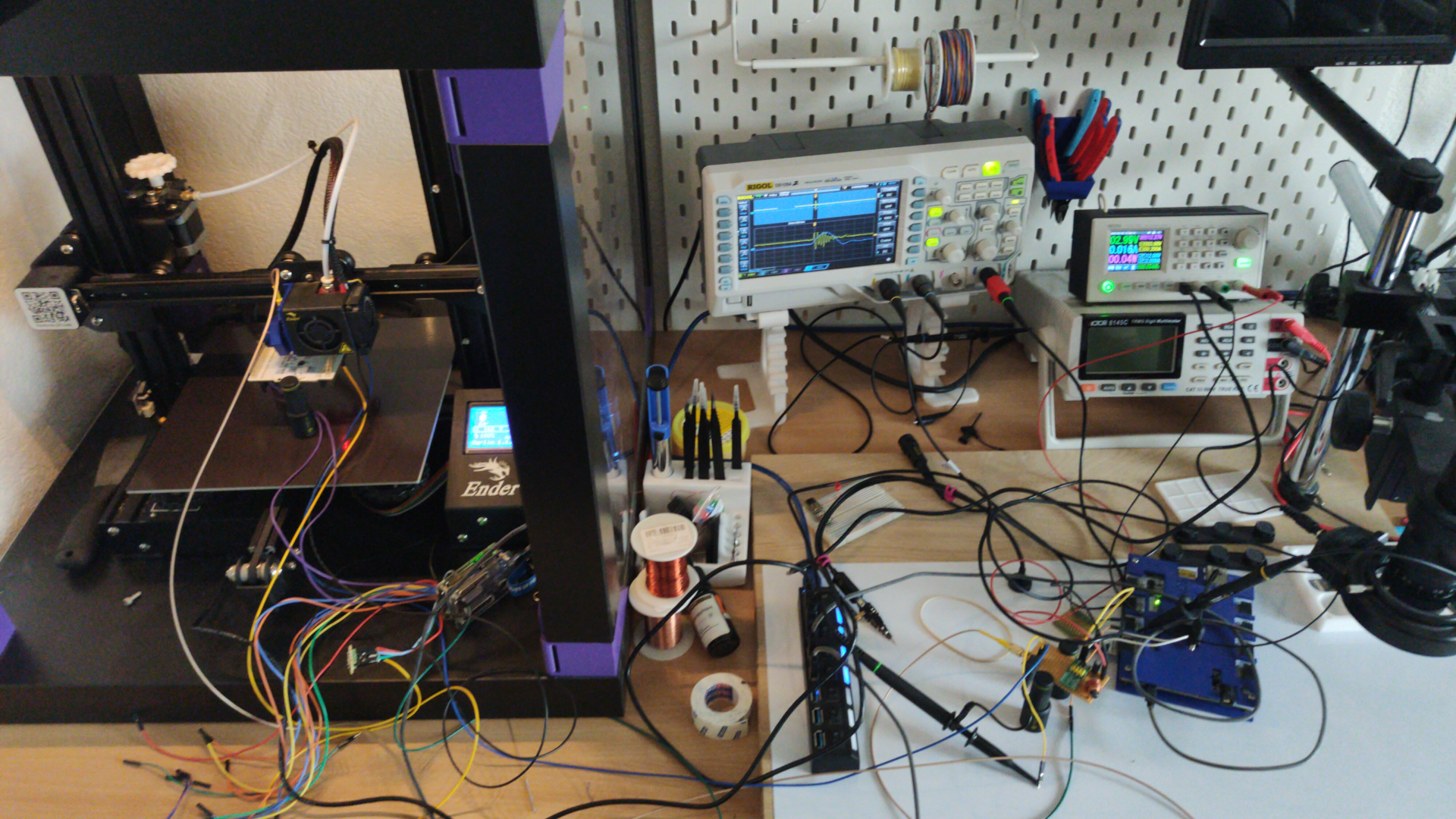
Final setup
Once everything is connected together, this huge mess of wires and probes is ready to be run.
Characterization
Test firmware
In order to detect faults and their effects, I prepared a very simple firmware in assembly that will trigger different debug breakpoints depending on the fault effect:
.thumb

@ Variables

.equ    RAM, (0x20000000)
.equ    RAM_END, (0x20010000)

@ Vector table start
.long               0x20001000  @SP value
.long               _start      @Reset
.long               _nmi        @NMI interrupt
.long               _hardfault  @Hard fault
.long               _memfault   @Memory fault
.long               _busfault   @Bus fault
.long               _usagefault @Usage fault
.long               0x00000000  @Reserved
.long               0x00000000  @Reserved
.long               0x00000000  @Reserved
.long               0x00000000  @Reserved
.long               0x00000000  @SvCall
.long               0x00000000  @Debug
.long               0x00000000  @Reserved
.long               0x00000000  @PendSV
.long               0x00000000  @Systick
@ Vector table end

.thumb_func
_start:
    MOV R2, #0
    LDR R3, =(RAM)
    STR R2, [R3]
    .thumb_func
    _loop:
        ADD R2, R2, #1
        LDR R1, [R3]
        ADD R1, R1, #1
        STR R1, [R3]
        CMP R1, R2
        BEQ _loop
    bkpt 0xb0
    b _start
.global _start

_nmi:
bkpt 0xa0
b _nmi

_hardfault:
bkpt 0xa1
b _hardfault

_memfault:
bkpt 0xa2
b _memfault

_busfault:
bkpt 0xa3
b _busfault

_usagefault:
bkpt 0xa4
b _usagefault
This firmware is a simple infinite loop that updates a register and a variable stored in SRAM synchronously. Both values are compared and if they differ somehow, a software breakpoint is raised.
I then used a Hydrabus as a SWD probe connected to the target in order to detect when the CPU stops its execution, retrieve the register status and the breakpoint code in order to know the kind of effect the fault triggered.
These helper functions were used to control and retrieve the status of the target CPU:
import pyHydrabus
s = pyHydrabus.SWD()

def init_swd():
    s.bus_init()
    s.read_dp(0)
    s.write_dp(4, 0x50000000)
    CSW = s.read_ap(0, 0)
    s.write_ap(0,0,CSW|0b10)

def halt_cpu():
    s.write_ap(0, 0x4, 0xE000EDF0) # DHCSR
    s.write_ap(0, 0xc, 0xA05F0003)

def run_cpu():
    s.write_ap(0, 0x4, 0xE000EDF0) # DHCSR
    s.write_ap(0, 0xc, 0xA05F0001)

def reset_cpu():
    s.write_ap(0, 0x4, 0xE000ED0C)
    s.write_ap(0, 0xc, 0x05FA0004)

def read_mem(address):
    s.write_ap(0, 0x4, address)
    return s.read_ap(0, 0xc)

def read_register(regnum):
    s.write_ap(0, 0x4, 0xE000EDF4) # DCRSR
    s.write_ap(0, 0xc, regnum)
    s.write_ap(0, 0x4, 0xE000EDF8) # DCRDR
    return s.read_ap(0, 0xc)

def write_register(regnum, value):
    s.write_ap(0, 0x4, 0xE000EDF8) # DCRDR
    s.write_ap(0, 0xc, value)
    s.write_ap(0, 0x4, 0xE000EDF4) # DCRSR
    s.write_ap(0, 0xc, regnum|1<<16)

def is_running():
    s.write_ap(0, 0x4, 0xE000EDF0)
    DHCSR = s.read_ap(0,0xc)
    return (DHCSR&0x20000) == 0
The most important part is in the run_cpu() function, where the C_DEBUGEN bit is set in the DHCSR register. That way the CPU will correctly halt at a bkpt instruction.
First scan
For each location on the die, two faults where generated per input voltage, and all the results where graphed based on the location and the type of fault. In this first scan, I used 0.2mm steps roughly across the center of the chip so I missed some regions on the edges of the die.
For instance, with 1V of input, the following faults were generated:

On the opposite, with 10V of input, way more faults are generated:

The labels are the following:
I performed the characterization with all voltages from 1 to 10 Volts in steps of 1V, and here are the results:

As we can see here, increasing the input voltage raises the chance that something bad happens. Looking back at the results, the highest successful glitch/voltage ratio is at 4 Volts, this is what we'll use for the next step.
Interestingly enough, no successful glitches were caused by a difference in the two register values. This either means there was an instruction skip or an instruction corruption.
RDP protection bypass
RDP is the flash readout protection for ST microcontrollers. Once set it prevents being able to read the flash memory from the bootloader or the debug interface. This protection has several levels depending on the MCU family. In this case, there is only one RDP level which prevents reading the flash but keeps the debug interfaces enabled.
We now know that the BBI can induce faults in the microcontroller. To make sure that this fault injection technique can be useful, let's try it on a more realistic scenario and try to reproduce the (in-)famous RDP bypass glitch but using BBI. This technique has been done several times using voltage glitch but as far as I know, never done using BBI.
The bypass vulnerability lies in the fact that the bootloader performs a software check in order to check if the flash content is locked or not, and a glitch can bypass this check:
After locking the flash using the ST utility or through the bootloader, the attack is quite simple:
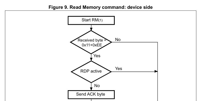
- Send the Read memory command (0x11, 0xEE)
- Send the glitch when the RDP check is done
- Flash memory is sent back by the bootloader.
Now that we fixed the gate pulse width and the voltage, only two parameters are still to be discovered: the delay after the command and the physical location of the injection on the die.
Bench setup
To prepare the target, I fixed BOOT0 to 1 and BOOT1 to 0 using jumpers so the board always starts in bootloader mode. I then used the following functions to interact with the UART interface:
def read_ack():
    ret = u.read(1)
    if ret == b'\x79':
        return True
    else:
        #print(f"Error {ret.hex()}")
        return False

def target_init():
    u.write(b'\x7f')
    i = 0
    while not read_ack() and i < 3:
        i = i+1

def target_lock():
    u.write(b'\x82\x7d')
    if not read_ack():
        #print("Error sending read command")
        return False
    else:
        return True

def target_program():
    u.write(b'\x31\xce')
    if not read_ack():
        print("Error sending write command")
        return None
    u.write(b'\x08\x00\x00\x00\x08')
    if not read_ack():
        print("Error sending address")
        return None
    u.write(b'\x06SUCCESS\x45')
    if not read_ack():
        print("Error sending data")
        return None

def target_read():
    u.write(b'\x11\xee')
    if not read_ack():
        #print("Error sending read command")
        return None
    u.write(b'\x08\x00\x00\x00\x08')
    if not read_ack():
        #print("Error sending address")
        return None
    u.write(b'\xff\x00')
    if not read_ack():
        #print("Error sending size")
        return None
    return u.read(256)
Using these helper functions, I can program and lock the flash with the following commands:
target_reset()
target_program()
target_lock()
target_read()
Glitch campaign
I then used the UART line to synchronize my FPGA with the Read memory command by counting the number of edges of the read memory command (0x11 0xEE). I can then start iterating through delays and die position:
for position in target.vertical():
    x,y = position
    ender.set_pos(x,y,UP)
    ender.set_pos(x,y,DOWN)
    for delay in range(1200,2000,10):
        bbi.delay = delay
        for _ in range(5):
            target_reset()
            bbi.arm()
            status = target_read()
            if status is not None:
                print(f"fault @ {ender.get_pos()} with {delay} delay")
                print(status)
                oscillo_screenshot(f"{x}-{y}-{delay}.png")
    ender.set_pos(x,y,UP)
And after some time, I finally got positive results:
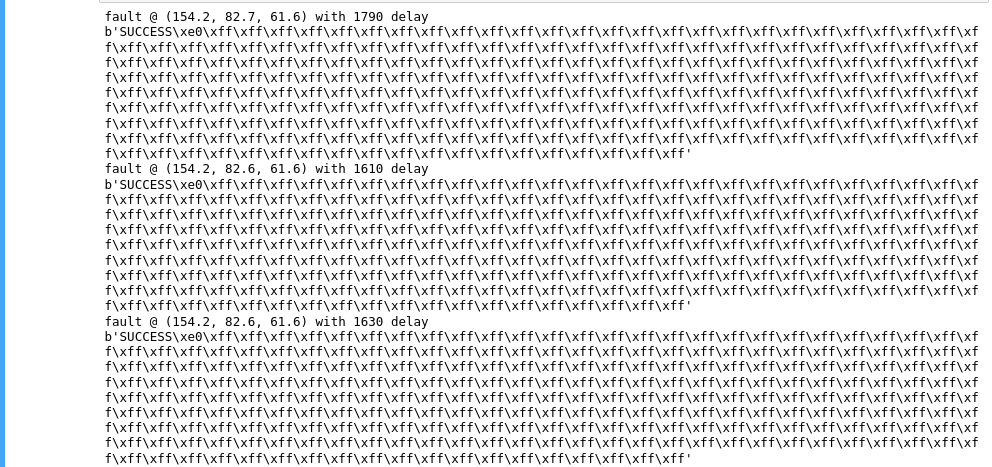
During the campaign, I also got several flash mass-erases which led to lots of false positives and a ruined night of sampling since the mass erase also clears the readout protection. I found out that the mass-erases happened around 3.5µs after the last rising edge of the UART line. The delay value (1790 for instance) are steps on the FPGA, which is clocked at 200MHz so about 8.95µs after the last rising edge of the UART line.
Note that the trigger is not perfectly aligned with the CPU execution, as there is several microseconds of jitter between the request and the response. This means that there could be some missing faults even if everything is correct. I could however get up to 3 faults at the same physical location out of 5 tries per location.
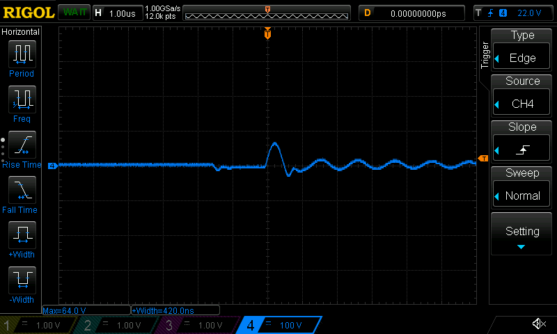
My script also takes oscilloscope screenshots of successful glitches. Here is one for reference:
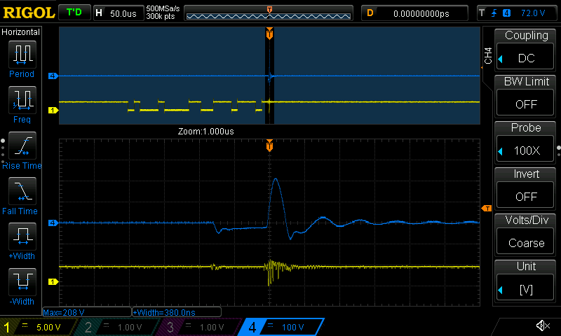
Yellow line is the UART, blue is the BBI probe voltage.
Analyzing results
Here is the plot of all successful RDP bypasses locations on the die:

But now, what is exactly causing the fault ? We are unfortunately not able to access the debug interface when in bootloader mode, so how can we know which component is vulnerable here ? Fortunately for me, I was able to use some tools at work to thin and polish the die and take infrared pictures to see the basic blocks within the die. I then mapped the plot and the resulting picture and got this:
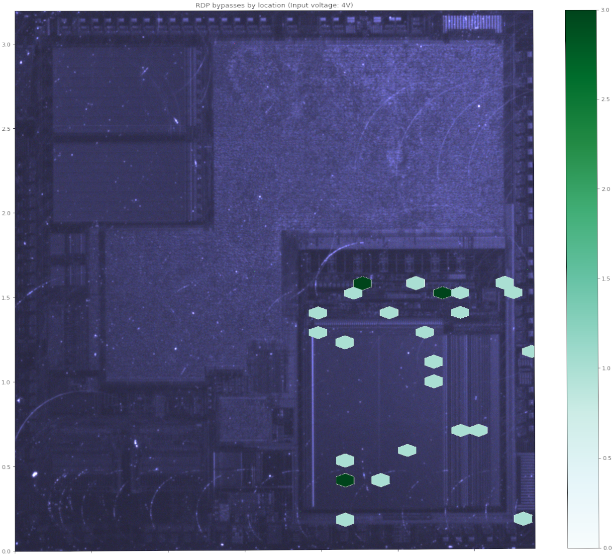
Even if the locations are not fully accurate, we can see that the flash memory (located on the lower right corner) is at fault. This means that we are faulting a flash read or register in order to bypass the RDP restriction. Interestingly enough, no CPU fault triggered the vulnerability (at least not with this input voltage).
Bootloader analysis
In order to analyze the results further, I dumped and analyzed the bootloader in order to see how the bootloader checks whether the RDP is enabled or not. After some time analyzing it, I located the following function:
┌ 14: fcn.1ffff132 ();
│           0x1ffff132      c049           ldr r1, [0x1ffff434]        ; [0x1ffff434:4]=0x40022000
│           0x1ffff134      0020           movs r0, 0
│           0x1ffff136      c969           ldr r1, [r1, 0x1c]
│           0x1ffff138      8907           lsls r1, r1, 0x1e
│       ┌─< 0x1ffff13a      00d5           bpl 0x1ffff13e
│       │   0x1ffff13c      0120           movs r0, 1
└       └─> 0x1ffff13e      7047           bx lr
The base register (0x40022000) is the flash controller base address. The code loads the register at address 0x4002201C and checks for the last two bits. Looking at the PM0075 document from ST shows that this is the FLASH_OBR register, and that the last two bits are:
- RDPRT - When set, this indicates that the Flash memory is read-protected
- OPTERR - When set, this indicates that the loaded option byte and its complement do not match.
All of this seems to make sense. The check is performed on a hardware flash controller register, this could explain why the successful faults are happening in the vicinity of the flash memory.
Conclusions
BBI is an interesting technique for sure. It offers the possibility to have a better spatial localization of the injected faults and provides a new way of injecting faults in a target at a reasonable cost.
However, this also comes with lots of drawbacks. The biggest one being the fact that the chip has to be prepared in order to access the silicon before being able to inject faults. The second drawback is the need for multiple tools and measurement probes in order to make sure that everything works the way it should. Adding the high voltage probes and the XYZ table into the bench setup is not an easy task and takes some time to setup correctly.
Compared to voltage glitching for instance, several other parameters have to be taken care of, such as the physical position of the injection probe and the input voltage. This makes the characterization way more challenging and time consuming.
It is nonetheless a different technique, and as such can be useful in some specific cases. The next step is to test BBI on devices protected by glitch detectors and see if it is possible to bypass this kind of protection.